Definition: The load line analysis of transistor means for the given value of collector-emitter voltage we find the value of collector current. This can be done by plotting the output characteristic and then determine the collector current IC with respect to collector-emitter voltage VCE. The load line analysis can easily be obtained by determining the output characteristics of the load line analysis methods.
DC Load Line
The DC load represents the desirable combinations of the collector current and the collector-emitter voltage. It is drawn when no signal is given to the input, and the transistor becomes bias.
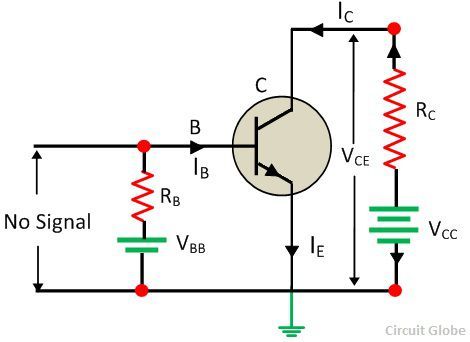
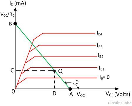
Consider a CE NPN transistor circuit shown in the figure below where no signal is applied to the input side. For this circuit, DC condition will obtain, and the output characteristic of such a circuit is shown in the figure below.
 The DC load line curve of the above circuit is shown in the figure below.
 By applying Kirchhoff’s voltage law to the collector circuit, we get,
 The above equation shows that the VCC and RC are the constant value, and it is the first-degree equation which is represented by the straight line on the output characteristic. This load line is known as a DC load line. The input characteristic is used to determine the locus of VCE and IC point for the given value of RC. The end point of the line are located as
1. The collector-emitter voltage VCE is maximum when the collector current IC = 0 then from the equation (1) we get,
 The first point A (OA = VCC) on the collector-emitter voltage axis shown in the figure above.
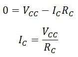
2. The collector current IC becomes maximum when the collector-emitter voltage VCE = 0 then from the equation (1) we get.
 This gives the second point on the collector current axis as shown in the figure above.
By adding the points A and B, the DC load line is drawn. With the help of load line, any value of collector current can be determined.

Good and valuable matter
marvelous explanation