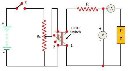
The volt-ampere characteristic of the PN-junction diode is a curve between the voltage over the junction and the circuit current. The circuit arrangement of the curve is shown in the figure below. The circuit arrangement shows that the resistor is connected in series with the PN junction diode to limit the forward bias current from rising within the permitted values. The characteristic curve of PN-junction diode is designed under three curves, i.e., zero external voltage, forward biasing, and reverse biasing.
 Zero External Voltage
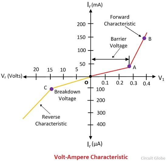
When the circuit K is open, no external voltage is applied to the circuit. Hence, no current flows in the circuit. The zero external voltage is shown by point O in the graph shown below.
Forward Biasing
The PN-junction diode is connected in forward biased by keeping the key K close and keeping the double throw switch in position one. In forward biasing the p-type semiconductor material connects to the positive end of the power supply and the n-type semiconductor material is connected to the negative terminal of the supply.
When the voltage is increased by varying the resistor value Rh, the circuit curve increases very slowly and the curve becomes non-linear. The point OA in the curve shown the increasing voltage characteristic.
The current slowly rises in the forward biasing because the applied external voltage is used to cross the potential barrier of the PN-junction diode. But when the potential barrier is completely eliminated, and the external voltage applies to the junction increases, the PN-junction behaves like an ordinary diode and circuit current increases sharply (shown in the region AB).
The increased circuit current is controlled by the resistance Rh and the junction forward resistance Rf. The curve becomes linear. The current exceed from rating value damage the diode.
The volt-ampere characteristic of PN Junction is shown in the figure below.
 Reverse Biasing
When the position of the double pole double throw switch changes from 1 to 2 the biasing of the diode becomes changes from reverse bias to forward bias, i.e., the p-type material connects to the negative terminal of the supply, and the n-type material is connected to the positive terminal of the supply.
Under reverse bias condition, the resistance of the diode becomes very high, and practically no current flows through the diode. But in actual practice current in milliamperes flow through the diode. This current is known as the reverse current. The reverse current is because of the minority charge carrier presents in the semiconductor material at normal room temperature. The reverse characteristic curve of PN-junction diode is shown in the figure above.
The reverse bias of the PN-junction act as a forward biased for majority charge carrier and hence they constitute a minority current in the reverse direction. This current is negligible over the working voltages.
When the reverse supply increases the reverse current also increases. The continuously increasing of reverse voltage increases the kinetic energy of the minority carriers. The kinetic energy of the minority electrons becomes so increases that they knock out the electrons from the semiconductor bond.
At this state the resistance of the barrier increases due to which breakdown occurs at the junction. Therefore the reverse biasing current increases and damage the junction permanently.
The voltage at which the PN-junction breaks is known as breakdown voltage.
The following are the important points taken into the considerations while plotting the volt-ampere characteristic curve.
- No current flows through the diode when the external voltage becomes zero.
- In forward bias, the current increase slightly till the depletion region is completely wiped off.
- The forward biased increases suddenly after the knee voltage.
- The forward current is limited by the series resistance R and the forward resistance Rf.
- The forward current increases beyond the rated value, destroy the diode.
- At reverse bias the reverse current increase slightly with the increase of a minority charge carrier.
- With the increase of the reverse voltage the reverse current increase abruptly to a large value. It is because of this voltage the junction of the transistor breaks and resistance fall suddenly.
The double pole double throw switch has two outputs (on and off) for each input.

It is a very good site that provided me with all the information l needed. Thanks.