The Avalanche Breakdown and Zener Breakdown are two different mechanisms by which a PN junction breaks. The Zener and Avalanche breakdown both occur in diode under reverse bias.
The avalanche breakdown occurs because of the ionisation of electrons and hole pairs whereas the Zener breakdown occurs because of heavy doping. These are explained below in details.
Avalanche Breakdown
The mechanism of avalanche breakdown occurs because of the reverse saturation current. The P-type and N-type material together forms the PN-junction. The depletion region develops at the junction where the P and N-type material contact.
The P and N-type materials of the PN junction are not perfect, and they have some impurities in it, i.e., the p-type material has some electrons, and the N-type material has some hole in it. The width of the depletion region varies. Their width depends on the bias applied to the terminal of the P and N region.
The reverse bias increases the electrical field across the depletion region. When the high electric field exists across the depletion, the velocity of minority charge carrier crossing the depletion region increases. These carriers collide with the atoms of the crystal. Because of the violent collision, the charge carrier takes out the electrons from the atom.
The collision increases the electron-hole pair. As the electron-hole induces in the high electric field, they are quickly separated and collide with the other atoms of the crystals. The process is continuous, and the electric field becomes so much higher then the reverse current starts flowing in the PN junction. The process is known as the Avalanche breakdown. After the breakdown, the junction cannot regain its original position because the diode is completely burnt off.
Zener Breakdown
The PN junction is formed by the combination of the p-type and the n-type semiconductor material. The combination of the P-type and N-type regions creates the depletion region.
The width of the depletion region depends on the doping of the P and N-type semiconductor material. If the material is heavily doped, the width of the depletion region becomes very thin.
The phenomenon of the Zener breakdown occurs in the very thin depletion region. The thin depletion region has more numbers of free electrons. The reverse bias applies across the PN junction develops the electric field intensity across the depletion region. The strength of the electric field intensity becomes very high.
The electric field intensity increases the kinetic energy of the free charge carriers. Thereby the carriers start jumping from one region to another. These energetic charge carriers collide with the atoms of the p-type and n-type material and produce the electron-hole pairs.
The reverse current starts flowing in the junction because of which depletion region entirely vanishes. This process is known as the Zener breakdown.
In Zener breakdown, the junction is not completely damaged. The depletion region regians its original position after the removal of the reverse voltage.
Equivalent Circuit of an Ideal Zener Diode and Actual Zener Diode
Ideal Zener Diode
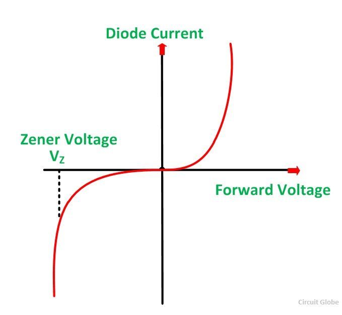
The breakdown region of the ideal Zener diode in the VI curve is considered to be vertical. The graph shows that the voltage remains constant even after the variation of the current.
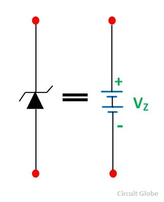
Thus, the resistance of the Zener diode is neglected. The Zener diode in the breakdown region ideally behaves like a battery.
The equivalent circuit diagram is shown below:
 In a circuit, an ideal Zener diode can be replaced by a voltage source Vz, when the Zener diode is operating in the breakdown region.
Actual Zener Diode
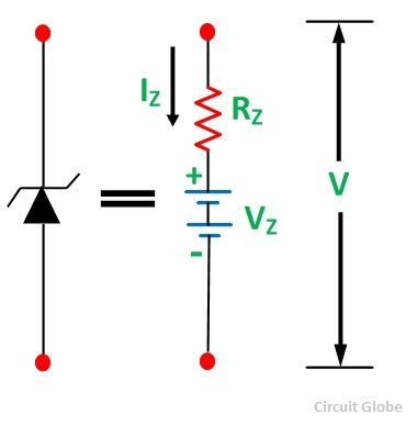
The breakdown region graph of the actual Zener diode is not accurately vertical. The graph shows that the Zener diode has some resistance.
The figure below shows that the Zener diode has some resistance Rz connected in series with the battery of voltage Vz.
 The voltage across the Zener diode will be:
This is all about Zener Breakdown and Avalanche Breakdown.


good explanation
good one
This is the best defination of values.
Thank you
Thank you
Excellent explanation
Tysm ❤️ the wordings you have used are so easy to know the working of zener diode and easy to learn. keep doing this for us
Simple language
Good explanation
Osm