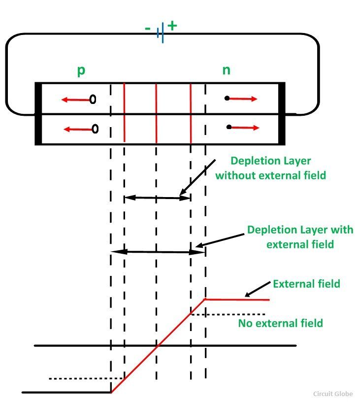
When the positive terminal of a DC source or battery is connected to n-type, and the negative terminal is connected to the p-type semiconductor of a p n junction, the junction is said to be in Reverse Biasing condition. The diagram of reverse bias p n junction is shown below.
In this case, the applied reverse potential acts in such a way that it establishes an electric field which increases the field due to the potential barrier. The potential barrier is thus strengthened. The increased potential barrier prevents the flow of majority charge carriers across the junction. Thus, a high resistive path is established by the junction, and practically no current flows through the circuit.
The external voltage applied to a p n junction that strengthens the potential barrier and prevents the flow of current through it is known as Reverse Biasing.
When the p n junction is reversed biased, the following points are concluded. They are as follows:-
- The potential barrier of the junction is strengthened.
- The junction offers high resistance to the flow of current, known as Reverse Resistance (Rr).
- Practically, no current flows in the circuit due to the establishment of a very high resistance path.
It is seen that practically no current flows through the junction, but a little amount of currents in microampere flows through the junction because of minority carriers available in the semiconductor. However, this current is neglected for all practical purposes.


good